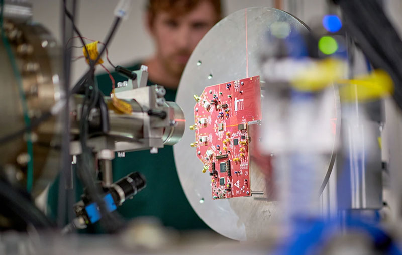
Michigan State University technology to further develop semiconductors

As we strive to pack ever smarter and more powerful electronics into ever smaller devices, one of the challenges is to develop tools and techniques that allow us to analyze the materials these devices are made of with ever greater precision.
Physicists at Michigan State University have taken a long-awaited step on this front with an approach that combines high-resolution microscopy with ultrafast lasers.
The described technique 8th of July in the Journal Nature Photonicsallows researchers to detect misplaced atoms in semiconductors with unprecedented precision. In semiconductor physics, these atoms are called “defects,” which sounds negative, but they are usually added to materials intentionally and are critical to the performance of semiconductors in current and future devices.
“This is particularly relevant for components with nanoscale structures,” says Tyler Cocker, Jerry Cowen Endowed Chair in Experimental Physics and leader of the new study.
This includes things like computer chips, which typically use semiconductors with nanoscale properties. And researchers are working to take nanoarchitecture to an extreme by developing materials that are just one atom thick.
Defects play a major role in electron movement, which is why scientists like Cocker are keen to know exactly where they are and how they behave. Cocker’s colleagues were excited to learn that his team’s new technique could easily provide them with this information.
“One of my colleagues said, ‘I hope you went out and celebrated,'” Cocker says.
Vedran Jelic, who led the project as a postdoctoral fellow in Cocker’s group and now works at the National Research Council Canada, is the first author of the new report. The research team also included doctoral students Stefanie Adams, Eve Ammerman and Mohamed Hassan, and undergraduate student Kaedon Cleland-Host.
Cocker adds that the technique is easy to implement with the right equipment, and his team is already applying it to atomically thin materials such as graphene nanoribbons.
“We have a number of open projects where we’re using the technique with more and more exotic materials,” says Cocker. “We’re basically integrating it into everything we do and using it as a standard technique.”
There are already tools, particularly scanning tunneling microscopes (STMs), that can help scientists detect individual atomic defects.
Unlike microscopes that many people are familiar with from science classes, STMs do not use lenses and light bulbs to magnify objects. Instead, STMs scan the surface of a sample with an atomically sharp tip, almost like the needle on a record player.
However, the tip of the STM does not touch the surface of the sample, it only comes close enough for electrons to jump or tunnel between the tip and the sample.
STMs record how many electrons jump and where they jump from, providing, among other information, information about samples at the atomic level (which is why Cocker’s lab calls it nanoscopy rather than microscopy).
However, STM data alone are not always sufficient to clearly detect defects within a sample. This is especially true for gallium arsenide, an important semiconductor material found in radar systems, high-efficiency solar cells and modern telecommunications equipment.
For their latest publication, Cocker and his team focused on gallium arsenide samples that were intentionally enriched with silicon defect atoms to optimize the movement of electrons through the semiconductor.
“The silicon atom basically looks like a deep pothole to the electrons,” says Cocker.
Although theorists have been studying these types of defects for decades, experimental physicists have not yet been able to directly detect these individual atoms.
Cocker and his team’s new technique still uses an STM, but the researchers also direct laser pulses directly at the tip of the STM.
These pulses consist of light waves at terahertz frequencies, meaning they wiggle up and down a trillion times per second. Recently, theorists had shown that this is the same frequency at which silicon atom defects in a sample of gallium arsenide should wiggle back and forth.
By coupling STM and terahertz light, the MSU team has developed a probe that has unprecedented sensitivity to the defects.
When the STM tip hit a silicon defect on the surface of the gallium arsenide, an intense signal suddenly appeared in the team’s measurement data. When the researchers moved the tip one atom away from the defect, the signal disappeared.
“Here was this defect that people had been looking for for over forty years, and we could see that it was ringing like a bell,” says Cocker.
“At first it was hard to believe because it was so obvious,” he continues. “We had to measure it in every way possible to make sure it was real.”
However, once the researchers were convinced that the signal was real, it was easily explained thanks to their years of theoretical work on the subject.
“When you discover something like this, it’s really helpful when there are already decades of theoretical research that thoroughly characterizes it,” says Jelic, who, along with Cocker, is also a corresponding author of the new paper.
Although Cocker’s lab is a leader in this field, there are groups around the world currently combining STMs and terahertz light. There are also a number of other materials that could benefit from this technique for applications beyond defect detection.
Now that his team has shared their approach with the community, Cocker is excited to see what other discoveries await.
The project was supported by the Office of Naval Research, the Army Research Office, and the Air Force Office of Scientific Research.


